Production Walkthrough
We collaborate with industry leaders to deliver cutting-edge PCB solutions and drive innovation in electronics manufacturing.
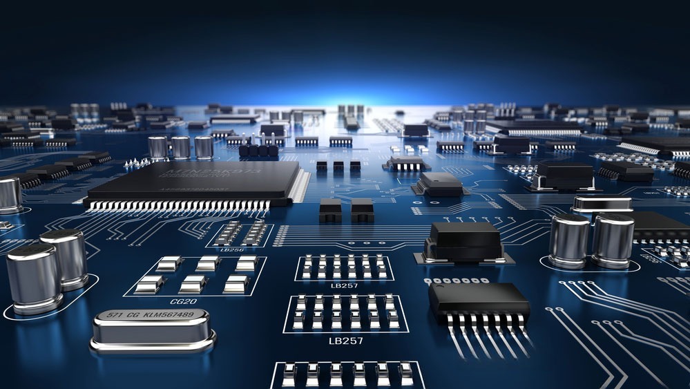
Complete PCB Production Walkthrough
1
PCB Fabrication (Creating the Bare Board)
PCB Fabrication Process
1.
Design and Preparation
- PCB Design: Engineers use CAD software (e.g., KiCad, Altium Designer) to create the circuit layout and schematic.
- Gerber File Creation: The design is exported into Gerber files, which are standard for PCB fabrication.
2.
Material Selection
- Substrate: Typically FR-4 (fiberglass-reinforced epoxy laminate) is used for rigidity and insulation.
- Copper Cladding: Thin layers of copper are laminated onto the substrate to form conductive pathways.
3.
Printing the Design
- Photoresist Application: A light-sensitive material (photoresist) is applied to the copper layer.
- Image Transfer: The design is projected onto the photoresist using UV light, hardening areas corresponding to the circuit traces.
- Etching: Unhardened photoresist is washed away, and unwanted copper is chemically etched to leave the desired circuit pattern.
4.
Layer Alignment and Lamination
- Multilayer PCBs: For multilayer boards, inner layers are aligned, bonded, and laminated under heat and pressure.
5.
Drilling
- Precise holes are drilled for vias, through-hole components, and mounting.
6.
Plating
- Holes are electroplated with copper to establish electrical connections between layers.
7.
Solder Mask Application
- A solder mask is applied to protect the copper traces and define areas for soldering.
8.
Silkscreen Printing
- Labels, logos, and component identifiers are printed on the board using silkscreening.
9.
Surface Finish
- Surface finishes (e.g., HASL, ENIG) are applied to protect exposed copper and enhance solderability.
10.
Testing
- The fabricated board undergoes electrical testing to check for shorts or open circuits.
2
PCB Manufacturing
Manufacturing Process
1.
Panelization
- Multiple PCB designs are arranged on a single panel for efficient manufacturing.
2.
Quality Control
- Each panel is inspected for alignment, trace accuracy, and surface integrity.
3.
Environmental Safety
- Waste materials like etching chemicals and unused copper are disposed of following environmental guidelines.
3
PCB Assembly (Adding Components)
Assembly Process
1.
Solder Paste Application
- Solder paste is applied to pads using a stencil to facilitate component soldering.
2.
Pick-and-Place Assembly
- Automated machines place surface-mount devices (SMDs) on the board with precision.
3.
Soldering
- Reflow Soldering: The board passes through a reflow oven to melt the solder and secure components.
- Wave Soldering: For through-hole components, boards are passed over a wave of molten solder.
4.
Inspection
- Automated Optical Inspection (AOI): Cameras verify the correct placement and soldering of components.
- X-Ray Inspection: Used for multilayer or densely populated PCBs to detect hidden defects.
5.
Manual Assembly
- For specialized components or low-volume boards, components may be added manually.
6.
Functional Testing
- The assembled board is powered and tested to ensure it functions as intended.
4
Final Steps
Completion Process
1.
Cleaning
- Any residual flux or contaminants are cleaned to ensure optimal performance.
2.
Packaging
- Boards are carefully packaged to prevent damage during transport and storage.
3.
Shipping
- The final product is sent to the customer or integrated into a larger system.